By Texas Instruments 114
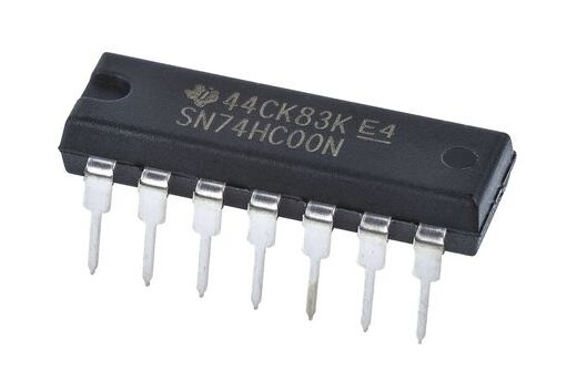
SN74HC00N is an integrated circuit chip belonging to the 74HC series. It uses CMOS technology and has the characteristics of high speed and low power consumption.
The SN74HC00N digital logic gate chip contains four independent 2-input NOR gates. It is mainly used for logical operations in digital circuits and can implement various logical functions, such as AND, OR, NOT, XOR, etc. The sn74hc00n digital logic gate chip has a wide operating voltage range, a wide operating temperature range, and a fan-out capability of up to 10 LSTTL loads.
Ⅰ.Specification parameters of SN74HC00N
•Number of circuits:4
•Number of digits:4 bit
•Number of inputs:2
•Logic function:NAND
•Product type:logic gate
•Logic series:HC
•Height:4.57 mm
•Length:19.3 mm
•Width:6.35 mm
•Number of gates:4 Gate
•Propagation delay time:8 ns
•Number of input lines:8 Input
•Number of output lines:4 Output
•Low level output current:5.2 mA
•High level output current:-5.2 mA
•Supply voltage-Maximum:6 V
•Supply voltage-Minimum:2 V
•Product:Single-Function Gates
•Minimum operating temperature:-40℃
•Maximum operating temperature:+85℃
•Package/Case:PDIP-14
•Function:Quad 2-Input
•Installation style:Through Hole
•Logic type:2-Input NAND
•Input type:Schmitt Trigger
•Output type:CMOS
•Operating power supply voltage:5 V
•Operating power supply current:20 uA
•Product type:Logic Gates
•Logic level-low:0.5V ~ 1.8V
•Logic level-high:1.5V ~ 4.2V
•Current-Quiescent (maximum):2 µA
•Maximum propagation delay at different V, maximum CL:15ns @ 6V, 50pF
Ⅱ.Functions and features of SN74HC00N
1.Input terminal characteristics: Each AND gate has two input terminals, allowing it to receive logic level signals. The input voltage range is wide and compatible with TTL and CMOS logic levels.
2.Logic function: Each SN74HC00N chip contains four independent two-input AND gates. The output of the AND gate is the result of the logical AND operation, that is, the output is high level only when all inputs are high level; otherwise, the output is low level.
3.Power supply characteristics: The SN74HC00N chip usually works on a 5V DC power supply, but it can also work on a 3.3V power supply.
4.Output terminal characteristics: Each AND gate has an output terminal, and the output terminal can provide the result of the corresponding input logic operation. The outputs can drive typical logic loads such as logic gates, flip-flops, etc.
5.Package form: SN74HC00N is usually packaged in DIP (Dual In-line Package), which is convenient for insertion into a standard breadboard or PCB for prototype design and production.
6.High-speed performance: Due to the use of CMOS technology, SN74HC00N has high speed and low power consumption. It is suitable for many high-speed digital logic applications.
Ⅲ.Application fields of SN74HC00N
1.Digital logic circuit design: As one of the basic logic gates, SN74HC00N can be used to design various digital logic circuits, such as counters, multiplexers, state machines, etc. For example, the SN74HC00N can be used to design a simple 2-bit binary counter. By properly connecting the input and output of the SN74HC00N, the addition or subtraction operation of the counter can be realized. The logic NOT gate of each SN74HC00N can perform a NOT operation on the two outputs of the counter, thereby realizing the inversion of the counter.
2.Sequential logic circuit: SN74HC00N can be used to build sequential logic circuits, such as flip-flops, clock dividers, etc., to process sequential signals and clock signals. These circuits are mainly used to process timing signals and clock signals to achieve signal synchronization and timing control.
3.Control system: In digital control systems, SN74HC00N can be used to implement logic control functions, such as signal processing, status judgment and control decision-making. In digital control systems, logic control functions are very important. As a basic logic gate, SN74HC00N can be used to implement various logic operations and control functions. For example, by appropriately connecting the inputs and outputs of the SN74HC00N, signal processing and transformation can be achieved. The input signal can be subjected to logical AND, OR, NOT and other operations, and then the operation results are output to the control system to realize control decisions and status judgments.
4.Communication system: In the communication system, SN74HC00N can be used to implement logical functions such as data demodulation, data encoding, and address resolution. Data transmission in communication systems usually requires a series of encoding and decoding processes to ensure correct transmission and reception of data. As a basic logic gate, SN74HC00N can be used to implement these encoding and decoding processes. For example, it can be used for data decoding to decode the received encoded data and restore it to the original data signal.
5.Data processing: In the field of digital signal processing, SN74HC00N can be used for data processing and logical operations, such as data selection, logical operations, data comparison, etc. SN74HC00N can be used to implement data selection function. By connecting multiple input signals to the input terminals of the SN74HC00N, one of the signals can be selected as the output as needed. This data selection function is very common in digital signal processing and enables the routing and transmission of data.
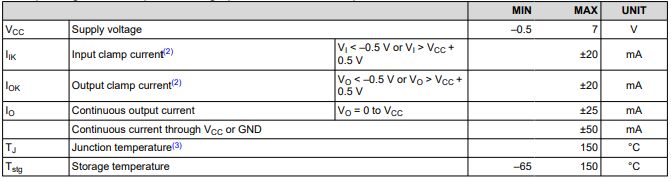
Ⅳ.Absolute Maximum Ratings of SN74HC00N
over operating free-air temperature range (unless otherwise noted)
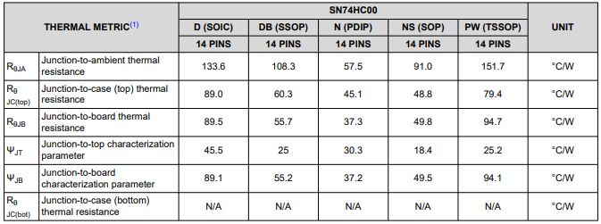
Ⅴ.Thermal Information of SN74HC00N
Ⅵ.Unique features of SN74HC00N
1.Low power consumption: Compared with LSTTL logic IC, SN74HC00N has lower power consumption. Due to the use of CMOS technology, its power consumption in the static state is very low, making it suitable for applications with higher power consumption requirements.
2.Noise tolerance: Due to the use of CMOS technology, SN74HC00N has good anti-interference ability and noise tolerance, and can work reliably in noisy environments.
3.Logic level compatibility: SN74HC00N is manufactured using CMOS technology, and its input and output levels are compatible with standard TTL (Transistor-Transistor Logic) logic levels, allowing it to be directly connected to TTL logic ICs without logic level conversion. device. The logic levels of LSTTL logic ICs may not be fully compatible with TTL logic, so additional level conversion circuits may be required in some applications.
4.Temperature stability: The working performance of SN74HC00N remains stable within a wide temperature range, and is suitable for situations where the working environment temperature changes greatly.
5.High-speed performance: SN74HC00N has a high operating speed and is suitable for high-speed digital logic circuit design. Compared with LSTTL logic IC, it has shorter transmission delay and faster response speed.
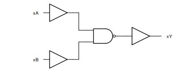
Ⅶ.Functional Block Diagram of SN74HC00N
Ⅷ.Replacement model of SN74HC00N
•CD74HC00E
•SN74HCT00N
•MC74HC00AN
•74LS00
•74HCT00D
Frequently Asked Questions
1.How many NAND gates are there in SN74HC00N?
SN74HC00N contains four NAND gates.
2.How many inputs does each logic gate of SN74HC00N have?
Each logic gate in the SN74HC00N has two inputs.
3.Is SN74HC00N compatible with CMOS logic levels?
Yes, SN74HC00N is compatible with CMOS logic levels.
4.What is the working principle of SN74HC00N?
The output signal of each AND gate is generated by logical operation based on the logic state of the input signal. The output terminal of SN74HC00N provides the output signal of the AND gate, which can be directly connected to other logic gates, flip-flops or loads.