By TI 3804
TL494 is an IC widely used in switching power supplies and other power management applications. It is a PWM controller mainly used to generate adjustable pulse signals to control the conduction time of power switching devices (such as MOSFETs) in switching power supplies to achieve stable regulation of the output voltage.
In a common voltage configuration, the error amplifier can compensate for voltages from -0.3 to VCC -2 volts. The comparator controls the dead time with a fixed offset. The dead time comparator provides almost 5% range. An external oscillator can also provide a reference frequency signal to this PWM. The user can bypass the on-chip oscillator by connecting RT to the reference output pin.
TL494 is a fixed frequency pulse width modulation circuit with a built-in linear sawtooth oscillator. The oscillation frequency can be adjusted through an external resistor and a capacitor. It is mainly designed for switching power supply controllers.
Ⅰ.Specification parameters of TL494
•Reference voltage:5V
•Working voltage:4V~40V
•PWM frequency range:between tens of kHz and hundreds of kHz
•Dead time control characteristics:variable range
•Selectable operation of dual outputs:single-ended or push-pull operation
•Operating temperature range:-40°C~85°C
•Sink and source current rating:200mA
•Pulse width modulation output:2
Ⅱ.Functional characteristics of TL494
1.Reference voltage source: TL494 integrates a stable reference voltage source internally, which is used to set the reference value of the output voltage. This helps achieve precise power regulation.
2.PWM control function: TL494 is mainly used to generate an adjustable PWM signal. By adjusting the width of the pulse (duty cycle), the output voltage of the switching power supply can be adjusted.
3.Error amplifier: TL494 contains an error amplifier to compare the difference between the output voltage and the reference voltage. This helps generate PWM signals to maintain output voltage stability.
4.Soft start function: TL494 supports soft start. By gradually increasing the output voltage, the impact of power supply startup can be reduced and the stability of the system can be improved.
5.Dead zone control: Dead zone control is to prevent power switching devices from being turned on at the same time, thereby reducing losses and horizontal stripes in the power supply. TL494 usually contains dead-time control circuitry inside.
6.External pins: TL494 usually has multiple pins, including PWM output pins, feedback pins, dead zone control pins, etc., to connect with external circuits and achieve flexible power supply design.
7.Frequency adjustment function: Users can adjust the frequency of the TL494 output pulse through external components (usually resistors or capacitors). This allows the TL494 to adapt to different application requirements.
8.Over-temperature protection: In order to prevent the chip from being damaged due to overheating, TL494 usually has an over-temperature protection function. Once the temperature exceeds the safe range, the chip takes steps to prevent further damage.
9.Overcurrent protection: TL494 usually has an overcurrent protection function, which can take measures to protect the power supply and related components when the output current exceeds the set value.
10.Wide operating voltage range: TL494 is usually able to operate within a relatively wide operating voltage range to adapt to different application scenarios.
Ⅲ.Working principle of TL494
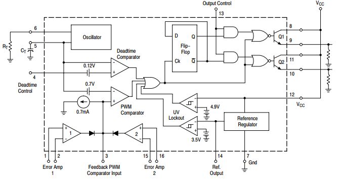
TL494 is a fixed frequency and variable duty cycle dual PWM control circuit. It doesn't require any external components to operate, except for some resistors and capacitors for the oscillator. This oscillator is responsible for generating the tooth lift wave based on the timing capacitor CT. The TL494 generates the signal by comparing the tooth waveform with two control signals from the error amplifier. When the sawtooth voltage is greater than the error amplifier output voltage, the output signal turns on. The working principle of TL494 involves several main parts, including error amplifier, comparator, sawtooth wave generator, dead zone control, output stage, etc. The basic working principle of TL494:
1.Feedback and Error Amplifier: An external feedback network compares the output voltage to a reference voltage and feeds the error signal into the error amplifier. The error amplifier amplifies this error signal and generates a voltage for comparison.
2.Sawtooth wave generator: TL494 contains a sawtooth wave generator internally, which generates a triangular waveform. This triangular waveform is the basis for the PWM signal.
3.Comparator: The generated error signal is sent to the comparator and compared with a triangle wave from the sawtooth wave generator. This comparison produces a pulse signal whose width depends on the size of the error signal.
4.Output stage: The PWM signal passes through the output stage and generates the corresponding output signal. The output stage generally includes one or more power switching devices (usually MOSFETs) used to control the power output.
5.Dead zone control: In order to prevent power switching devices from being turned on at the same time, dead zone control is introduced, that is, after one switch is turned off, wait for a period of time before turning on another switch. This prevents horizontal streaks and increases the efficiency of the system.
Ⅳ.Maximum Ratings of TL494
(Full operating ambient temperature range applies,unless otherwise noted.)

Maximum ratings are those values beyond which device damage can occur.Maximum ratings applied to the device are individual stress limit values (not normal operating conditions) and are not valid simultaneously. If these limits are exceeded, device functional operation is not implied, damage may occur and reliability may be affected.
Ⅴ.Adjust the parameters of TL494 to optimize the efficiency of the power supply
1.Optimize the duty cycle: Adjusting the duty cycle of the PWM signal can affect the turn-on and turn-off times of the power switching device, thus affecting the efficiency. Select an appropriate duty cycle to make the power switching device operate at the optimal operating point while avoiding dead zone problems.
2.Adjust the PWM frequency: Lowering the PWM frequency can reduce switching losses, but it will increase the size and weight of the output filter components. Choose an appropriate PWM frequency to balance switching losses and output filtering requirements.
3.Minimize switching losses: Reducing the turn-on and turn-off losses of power switching devices is the key to improving efficiency. This can be achieved by selecting power switching devices with low turn-on and turn-off losses, and optimizing dead-band control.
4.Optimize the feedback network: Properly designing the feedback network can ensure the stability of the output voltage and reduce the power consumption of the error amplifier.
5.Use efficient output filters: Choosing efficient output filter components, such as inductors and capacitors, can reduce output ripple and improve overall efficiency.
6.Choose high-efficiency components: Choosing high-efficiency components, such as power switching devices with low conduction and turn-off losses, and low-power external components can help improve overall efficiency.
7.Reduce static power consumption: When the power supply is in light load or standby state, the overall efficiency is improved by reducing the static power consumption of the power supply. This can be achieved by properly designing the soft-start circuit and introducing low-power modes.
8.Thermal management: Ensure that the heat dissipation design of the power supply is effective enough to prevent the chip from overheating, which in turn affects efficiency.
Ⅵ.Application fields of TL494
1.Switching power supply: TL494 is a PWM (Pulse Width Modulation) controller that is commonly used to design various switching power supplies, including switching power adapters, DC-DC converters and switching regulated power supplies. It can achieve precise regulation of the output voltage through PWM control. PWM control is a method of controlling the output voltage by adjusting the pulse width. In switching power supply design, the PWM controller is used to adjust the on-time of the switch to control the amplitude of the output voltage. In this way, precise voltage regulation can be achieved with the advantages of high efficiency and high reliability.
2.Battery charger: TL494 can be used to design battery chargers. Through PWM control, the charging current and voltage can be accurately adjusted to ensure efficient charging of the battery. In battery charger design, the advantage of a PWM controller is that it can achieve precise control of the battery charging process. By adjusting the duty cycle of the PWM signal, the size of the charging current and the length of the charging time can be controlled, thereby realizing the automation and intelligence of the charging process.
3.Inverters and frequency converters: TL494 can be used to control inverters and frequency converters, convert DC power to AC power, and achieve variable frequency output.
4.Motor drive: TL494 is a PWM controller that is often used in motor control circuits. By adjusting the duty cycle of the PWM signal, the speed and torque of the motor can be controlled. In motor control circuits, the TL494 is usually connected between a power supply and a motor. The power supply provides the required voltage to the TL494, and the motor is the controlled object. The comparator inside the TL494 can compare a reference voltage with a sawtooth wave voltage to generate a PWM signal.
5.Power inverter: In the power inverter, TL494 can convert a DC voltage into an AC voltage to meet the power needs of different devices. This conversion is done by inputting DC voltage to the input terminal of TL494, and then converting the DC voltage into AC voltage through the switching operation of the internal circuit, and outputting it to the power port of the device. Compared with other inverter technologies, inverters using TL494 have the advantages of small size, light weight, and low cost. In addition, the TL494 has built-in protection functions to protect the circuit safety of the inverter and equipment.
6.Inverter welding machine: Inverter welding machine usually requires precise PWM control to achieve a stable welding process, and TL494 can play a role in this regard.
Ⅶ.Working parts and principles of TL494
1.5V reference source
TL494 has a built-in reference source based on the band gap principle. The stable output voltage of the reference source is 5V, provided that the VCC voltage is above 7V and the error is within 100mV. The output pin of the reference source is pin 14 REF.
2.Operational amplifier
The TL494 integrates two single-supply operational amplifiers. The operational amplifier transfer function is ft(ni,inv)=A(ni-inv), but it cannot exceed the output swing. In general power circuits, the op amp is connected to operate in a closed loop. In a few special cases, open loop is used and signals are input from the outside. The output terminals of the two op amps are each connected to a diode, which is connected to the COMP pin and the subsequent circuit (comparator). This ensures that the higher output of the two op amps enters the subsequent circuit.
3.Sawtooth wave oscillator
TL494 has a built-in linear sawtooth wave oscillator, which generates a sawtooth waveform of 0.3~3V. The oscillation frequency can be adjusted through an external resistor Rt and a capacitor Ct. The oscillation frequency is: f=1/RtCt, where the unit of Rt is ohms and the unit of Ct is farad. The sawtooth wave can be measured at the Ct pin.
4.Quiet zone time comparator
The dead zone (literal translation dead zone) time is set by Dead Time Control pin 4, which interferes with the pulse trigger through a comparator and limits the maximum duty cycle. The upper limit of the duty cycle that can be set at each end is up to 45%. When the operating frequency is higher than 150KHz, the upper limit of the duty cycle is about 42%. (When the DTC pin level is set to 0).
5.Comparator
The signal output by the operational amplifier (COMP pin) enters the positive input terminal of the comparator inside the chip and is compared with the sawtooth wave entering the negative input terminal. When the sawtooth wave is higher than the signal at the COMP pin, the comparator outputs 0, otherwise it outputs 1.
6.Pulse trigger
The pulse flip-flop turns on when the comparator outputs 1 on the falling edge of the sawtooth wave, causing one of the two output terminals (in turn) to turn on the on-chip transistor, and turns off when the comparator output drops to 0.
Ⅷ.Pin distribution of TL494
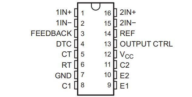
•Pin1(1IN+): This pin is generally used for voltage sampling of subsequent circuits.
•Pin2(1IN-): This pin is used for output voltage adjustment. Adjusting the potentiometer can control the output voltage
•Pin3(FEEDBACK): This pin is connected to the same pin of the "PWM" comparator inside the chip.
•Pin4 (DTC): Used for soft start to prevent the maximum voltage from being output as soon as power is turned on.
•Pin5(CT): Used to adjust the switching frequency. The voltage during normal operation is about 1.5V
•Pin6(RT): Used to adjust the switching frequency. The voltage during normal operation is about 3.5V
•Pin7(GND): Used for power supply ground pin
•Pin8(C1): Collector pin of output 1
•Pin9(E1): Emitter pin of output 1
•Pin10(E2): Emitter pin of output 2
•Pin11(C2): Collector pin of output 2
•Pin12(VCC): Positive power supply pin
•Pin13(OUTPUT CTR): Select output mode from three options
•Pin14(REF): 5V reference regulator output
•Pin15(2IN-): This pin is used to limit the maximum current by comparing it with the feedback voltage of pin 16
•Pin16 (2IN+): This pin is generally used for the voltage feedback value of the current sensing resistor current sampling of the subsequent circuit.
Frequently Asked Questions
1.What is the function of TL494?
The TL494 device provides for push-pull or single-ended output operation, which can be selected through the output-control function. The architecture of this device prohibits the possibility of either output being pulsed twice during push-pull operation.
2.What are the basics of TL494?
The TL494 uses a PWM control circuit to regulate power. It receives an input, compares it to a reference voltage, and then generates a pulse of varying width based on this comparison. This pulse is used to control the power in various electronic devices.
3.How does TL494 generate PWM signals?
TL494 generates PWM signals by comparing a reference voltage with the feedback voltage derived from the output. The error amplifier amplifies the difference, and this signal is compared with a sawtooth waveform to produce a PWM output.
4.What is the maximum frequency of TL494?
TL494 IC is a multifunctional single-chip PWM control circuit. This calculator will help you calculate the oscillator frequency based on a set of RC values or calculate the RC values based on a set of frequencies. The oscillator is programmable from 1kHz to 300kHz.
5.What is the feedback pin of TL494?
The feedback pin is the output of the two error amplifiers and is used to compare and adjust the output pulse width to the DC control voltage. The gain appears to be set to 101, using 51k feedback and a 2.5V reference resistor with a resistor of 510 ohms. It is used to control the gain of the feedback voltage.