By Texas Instruments 161
SN74LS00N is a digital integrated circuit that is part of the 74LS series (Low-Power Schottky series) produced by Texas Instruments. It is a Quad 2-input NAND gate, which means it has four input pins and one output pin, and the output is the result of the four-input NAND logic operation.
The 74LS series uses Schottky technology to reduce power consumption and increase operating speed. This chip is generally used in the design of digital logic circuits based on "NAND" logic gates. The output of the gate is logic high when all inputs are logic high, otherwise it is logic high. In this way, SN74LS00N can be used to implement various digital logic functions and circuits such as combination and sequence.

Ⅰ.Specification parameters of SN74LS00N
•Product type:logic gate
•Number of pins:14
•Maximum high-level output current:-0.4mA
•Product:Single-Function Gates
•Logic function:NAND
•Number of gates:4 Gate
•Logic series:LS
•Number of output lines:4 Output
•Number of input lines:8 Input
•Low level output current:8 mA
•High level output current:-400 uA
•Propagation delay time:10 ns
•Minimum operating temperature:0℃
•Maximum operating temperature:+70℃
•Supply voltage-minimum:4.75 V
•Supply voltage-Max:5.25 V
•Package/Case:PDIP-14
•Installation style:Through Hole
•Function:NAND
•Input type:TTL
•Height:4.57 mm
•Length:19.3 mm
•Width:6.35 mm
•Operating power supply voltage:5 V
•Operating power supply current:22 uA
•Logic type:2-Input NAND
•Logic level-low:0.8V
•Logic level-high:2V
•Maximum propagation delay at different V, maximum CL:15ns@5V, 15pF
Ⅱ.Environmental and export classification of SN74LS00N
•Properties:Description
•ECCN:EAR99
•HTSUS:8542.39.0001
•REACH status:non-REACH product
•RoHS status:complies with ROHS3 specifications
•Moisture Sensitivity Level (MSL):Not applicable
Ⅲ.Pin configuration of SN74LS00N
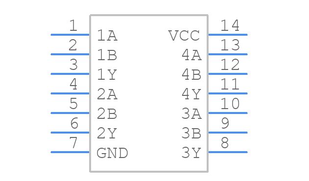
•Pin1,2,4,5(1A,2A,4A,5A): These are the four input pins. Each input can accept a logic high or logic low signal.
•Pin3(1Y): This is the output pin that provides four inputs for logical NAND operations. The output signal is logic low when all inputs are logic high and logic high otherwise.
•Pin6(4Y): This pin is usually marked as "NC" (No Connection), indicating that it is not connected to the internal circuit of the chip. There may be no connected pins in some packages.
•Pin7(GND): This is the ground pin, connected to the ground of the circuit.
•Pin8,9,10,11,12,13(NC): These pins are marked "NC" (No Connection), indicating that they are not connected to the chip's internal circuitry. In some packages, these pins may not be connected to the chip's internal circuitry.
•Pin14(VCC): This is the positive power pin, connected to the positive power supply of the circuit.
Ⅳ.Absolute Maximum Ratings of SN74LS00N
over operating free-air temperature range(unless otherwise noted)
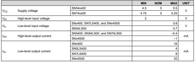
Ⅴ.Recommended Operating Conditions of SN74LS00N
over operating free-air temperature range(unless otherwise noted)
Ⅵ.Application fields of SN74LS00N
1.Combinational logic circuit: SN74LS00N is a four-channel positive input NAND gate. A NAND gate is a logic gate whose output is true only when all inputs are true. The output of a NAND gate in the truth table is "false" (0) if and only if all inputs are "true" (1). In combinational logic circuit design, NAND gates are often used as the basic building blocks to implement various logic functions. For example, a binary adder can be easily implemented using NAND gates. In binary addition, the result bit is 0 (equivalent to the output of a NAND gate) only if all input bits are 1. Therefore, full adders can be implemented by using NAND gates, which can further be combined to implement more complex arithmetic circuits such as full subtractors, binary multipliers, etc.
2.Control system: SN74LS0ON is a four-way forward NAND gate integrated circuit. It is usually used in digital logic control systems to perform various logical operations, coordinate and manage various signals in the system. This kind of integrated circuit is widely used in digital control systems such as industrial control, electronic instruments, and computer hardware. For example, in the control system of CNC machine tools, SN74LS0ON can be used to implement various logic controls, such as tool selection, cutting feed, coolant switch, etc. In other types of digital control systems, it can also be used to process Various switching inputs and outputs enable complex logic control.
3.Communication system: In digital communication systems, SN74LSOON can be used to process and manage digital signals, perform logical operations, and control data flow. These functions mainly rely on various logical operations implemented by its internal forward NAND gates. When designing and applying SN74LS0ON, key factors that need to be considered include its input and output voltages and levels, logic gate response time, power consumption, thermal design, etc. At the same time, attention must also be paid to its driving capability and interface compatibility to ensure its Can effectively function in communication systems.
4.Sequential circuit: SN74LS0ON is a four-way forward dual-input NAND gate. In sequential circuits, it can be used to build various sequential logic elements, such as flip-flops and counters. This is because NAND gates are very useful in time logic designs because they have the property of retaining their last state until a new input signal is received. A simple flip-flop can be built using the SN74LSOON. A flip-flop is a storage element that changes state when it receives an input signal. With NAND gates, you can connect two input signals to one NAND gate and then feed the output back to the other input. When the input signal changes, the output state remains unchanged until the next input signal change.
5.Instrumentation: In test and measurement instruments, SN74LS00N can be used to implement various digital logic functions, such as data processing and signal processing.
6.Microprocessor system: SN74LS00N is often used to implement input/output port control and logic operations in microprocessor and microcontroller systems. This is mainly due to its logic functions, especially the functions of NAND gates. Input/output ports in microprocessor and microcontroller systems are usually required to perform various logical operations such as AND, OR, NAND, and NOR, etc. These operations can be used to control and operate the device or system connected to the port.
Ⅶ.SN74LS00N method of realizing logic gate combination
1.Four-input NAND operation: The main logic function of SN74LS00N is to perform four-input NAND operation. The level of the output pin (1Y) depends on the levels of the four input pins. Specifically, the output is logic low only when all input pins are logic high, otherwise it is logic high. .
2.Connect the input pins: Connect the signals to be operated logically to the input pins of SN74LS00N (1A, 2A, 3A, 4A). This can be a logic high (+5V) or logic low (0V) signal.
3.Observe the output pin: Connect to the 1Y pin and observe the output signal. According to the logic operation of NAND gates, when all inputs are logic high, the output is logic low, otherwise it is logic high.
Frequently Asked Questions
1.What is the output capability of SN74LS00N?
The output capability of SN74LS00N refers to the characteristics of the current and voltage it can output. At IOH=-400μA, the typical value is above 2.7V. This means that at an output current of -400μA, the output voltage is higher than 2.7V. When IOL=4mA, the typical value is below 0.5V. This means that when the output current is 4mA, the output voltage is less than 0.5V. At VOH=2.7V, the typical value is -400μA. This means that when the output voltage is 2.7V, the maximum output current is -400μA. At VOL=0.5V, the typical value is 4mA. This means that when the output voltage is 0.5V, the maximum output current is 4mA.
2.What should you pay attention to when connecting SN74LS00N to other ports of the microprocessor?
Pay attention to the output capabilities of the SN74LS00N and ensure that the connected load does not exceed its specifications. If desired, a current amplifier or buffer can be added to increase the output capability. If there are timing relationships with other ports on the microprocessor, ensure that the signals and clocks are properly synchronized. Flip-flops or other timing elements may be required to ensure the correct sequence of operations.
3.Are there any alternative models or chips with similar functions to SN74LS00N?
Alternative models of SN74LS00N include: SN74LS00D, SN74LS02N, SN74HC00N, 74HCT00N, SN74LS08N, etc.