By ON Semiconductor 1063
MTB30P06VT4G is a P-channel field effect transistor (P-channel MOSFET), which is a common electronic device and is widely used in power switches and amplifier circuits.
The P-channel field effect transistor is a voltage-controlled device whose working principle is based on the electric field effect to control the on-off current. The main parameters of MTB30P06VT4G include rated voltage, rated current, on-resistance, etc. In practical applications, it is necessary to select the appropriate field effect transistor model according to the specific requirements of the circuit and ensure that its parameters meet the circuit requirements.
Ⅰ.Factors to consider when using MTB30P06VT4G as a power switch or amplifier appliance
1.Rated voltage: The rated voltage of the field effect transistor needs to be selected according to the maximum voltage of the circuit, ensuring that it is greater than the maximum voltage of the circuit.
2.On-resistance: The smaller the on-resistance, the smaller the conduction loss of the field effect transistor and the higher the efficiency. Therefore, when selecting a field effect transistor, you should try to choose a model with a smaller on-resistance.
3.Rated current: The rated current of the field effect transistor needs to be selected according to the maximum current of the circuit to ensure that it can withstand the maximum current of the circuit.
4.Switching speed: For circuits that require fast switching, field effect transistors with faster switching speeds should be selected.
5.Package form: The appropriate package form needs to be selected according to the size and heat dissipation requirements of the circuit.
Ⅱ.Main parameters of MTB30P06VT4G
•FET type:P channel
•Product type:MOSFET
•Installation style:SMD/SMT
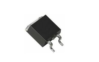
•Package/Box:D2PAK-3(TO-263-3)
•Transistor polarity:P-Channel
•Number of channels:1 Channel
•Vds-drain-source breakdown voltage:60 V
•Id-continuous drain current:30 A
•Rated voltage (DC):-60.0V
•Rated current:-30.0A
•Drain-source resistance:80mΩ
•Vgs-gate-source voltage:-15V, +15V
•Minimum operating temperature: -55℃
•Maximum operating temperature:+175℃
•Power dissipation:3W
•Drain-source voltage (Vds):60V
•Drain-source breakdown voltage:60V
•Gate-source breakdown voltage:±15.0V
•Continuous drain current(Ids):30.0A
•Pd-Power dissipation:3W
•Rise time:25.9ns
•Fall time:52.4 ns
•Packaging:Reel/Cut Tape/MouseReel
•Configuration:Single
•Input capacitance(Ciss):2190pF @25V(Vds)
•Rated power(Max):3W
•Forward transconductance - minimum:7.9S
•Typical shutdown delay time:98ns
•Typical turn-on delay time:14.7ns
•Height:4.83mm
•Length:10.29mm
•Current at 25°C-Continuous Drain (Id):30A (Tc)
Ⅲ.Thermal characteristics of MTB30P06VT4G
The thermal characteristics of the MTB30P06VT4G depend on its operating conditions and environment. As a semiconductor device, MTB30P06VT4G generates heat when working, and its thermal characteristics are closely related to circuit design and application environment. In order to ensure the stability and reliability of MTB30P06VT4G, the following thermal-related factors need to be considered:
1.Operating temperature range: The operating temperature range of MTB30P06VT4G is generally between -55℃ and 150℃. When selecting and using, ensure that its operating temperature is within the range specified in the device's specifications to avoid overheating or overcooling that may affect its performance and reliability.
2.Heat dissipation design: Choose the appropriate heat dissipation or heat dissipation method for MTB30P06VT4G, such as natural heat, forced air cooling or liquid cooling, etc. Heat sink selection should consider factors such as its thermal resistance, weight, and cost.
3.Junction temperature: The junction temperature of MTB30P06VT4G should be kept within the range specified in the specification. Excessive junction temperature may cause device performance degradation or damage, so the circuit design, working conditions and usage environment need to be evaluated to ensure that the junction temperature Within reason.
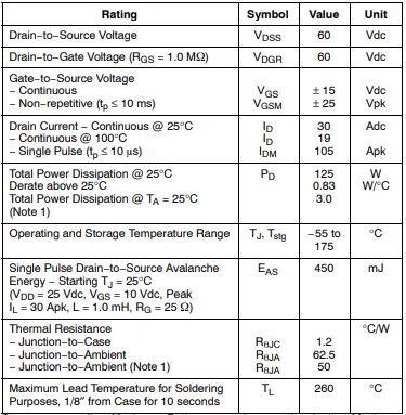
Ⅳ.Maximum Ratings of MTB30P06VT4G( (TC=25°C unless otherwise noted))
Ⅴ.Application fields of MTB30P06VT4G
1.Inverter: used in inverter circuits to convert DC power into AC power. Inverters are commonly used in solar power generation, power transmission and power electronics applications.
2.Power switch: P-channel MOSFET is often used in power switch circuits to control the on and off of DC power supply. This device enables efficient power control in power management circuits.
3.Switching power supply: P-channel MOSFET can be used in switching power supplies to control power output and improve power efficiency and stability.
4.Power amplifier: P-channel MOSFET can be used in the output stage of the power amplifier to control and amplify electrical signals. This may be common in audio, RF, and other signal amplification applications.
5.Power inverter: used in automotive electronics, solar inverters and other applications that need to convert electrical energy from DC to AC.
6.Motor drive: used in motor drive circuits, especially applications that need to control the start, stop and speed of the motor. P-channel MOSFETs can play an important role in motor control.
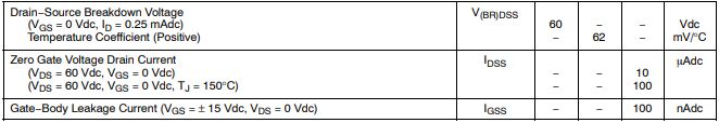
Ⅵ.OFF Characteristics of MTB30P06VT4G
Ⅶ.Precautions for MTB30P06VT4G
1.Polarity: Make sure to connect the various pins of the device correctly to avoid damage. Pay special attention to the correct connections of source, drain and gate.
2.Electrostatic protection: Take appropriate electrostatic protection measures to prevent damage to devices caused by electrostatic discharge.
3.Maximum ratings: Do not exceed the maximum ratings of the device, such as maximum drain-source voltage (VDS) and maximum drain current (ID). Exceeding these values may cause device damage.
4.Over-current and over-temperature protection: Over-current protection and over-temperature protection circuits may need to be considered in the circuit to ensure protection of the MTB30P06VT4G under abnormal conditions.
5.Temperature range: Ensure operation within the specified operating temperature range of the device. Exceeding the specified temperature range may affect performance or cause malfunction.
6.Heat dissipation: For high-power applications, appropriate heat dissipation design should be considered to ensure that the device operates within the allowed temperature range.
7.Impedance matching: Ensure the impedance matching of MTB30P06VT4G in the circuit to prevent reflection and improve efficiency.
Ⅷ.Replacement model of MTB30P06VT4G
1.IRF4905: Provided by International Rectifier, suitable for power switching and power management applications.
2.SI2319DS: Provided by Vishay Company, widely used in power management and switching power supply applications.
3.SUP75P03-07: Provided by Vishay Company, suitable for applications such as power switches and power amplifiers.
4.AO3401A: Provided by Alpha & Omega Semiconductor (AOS), used for power management and power switching circuits.
Frequently Asked Questions
1.How to reduce the on-resistance of MTB30P06VT4G?
The on-resistance of a MOSFET is usually related to the current when it is turned on. Increasing drive current can help reduce on-resistance. Make sure the driver circuit can provide enough current to ensure the MOSFET is in its optimal operating condition. In high-power applications, using a low-resistance heat sink can help lower the operating temperature of the MOSFET, thereby reducing the on-resistance. Effective thermal design is critical to keeping temperatures down.
2.What packages are available for MTB30P06VT4G?
TO-220, TO-252 (DPAK), TO-263 (D2PAK)
3.What is the working principle of MTB30P06VT4G?
In the conduction state, when sufficient positive voltage is applied to the gate, the P-channel MOSFET enters the conduction state. In this state, a conductive channel is formed between the source and drain, through which current can flow. Current flows from source to drain and is controlled by applying a voltage to the gate. In the cut-off state, when a low voltage or zero voltage is applied to the gate, the P-channel MOSFET enters the cut-off state, the conductive channel is closed, and current cannot flow through it. This achieves a controllable current on-off switch.