By Texas Instruments 175
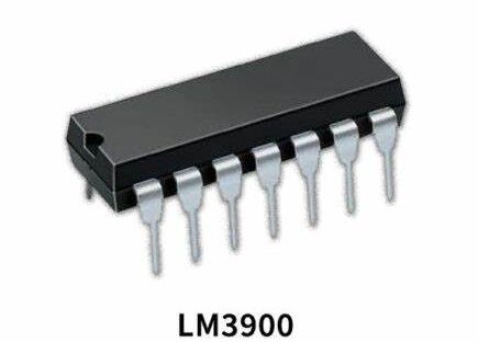
The LM3900 series includes four separate, two-input built-in compensation amplifiers designed for a single supply voltage and a large output voltage swing. This circuit uses a current mirror to complete the inverting input function. Suitable for AC amplifiers, active filters, low-frequency triangle waves, square waves, pulse waveform generation circuits, speedometers, low-voltage digital logic gates, etc.
Ⅰ.Working principle of LM3900
1.Differential input: The operational amplifier has two input terminals, namely the non-inverting input terminal (+) and the inverting input terminal (-). In differential input mode, the op amp attempts to equalize the voltage at these two inputs.
2.Feedback: In order to stabilize the operation of the operational amplifier, a feedback circuit is usually used. The feedback circuit feeds part of the output voltage back to the input to suppress erratic op amp behavior. Common types of feedback include positive feedback and negative feedback.
3.High gain: One of its important features is its high gain. When there is a small difference in voltage at the differential input, the op amp circuit will amplify the difference and try to form a voltage on the output that reduces the differential input voltage.
4.Input current of the op amp: The LM3900 has an input current, often called input bias current. This refers to the tiny current introduced by the nature of the semiconductor material that flows into or out of the input of the op amp.
5.Supply voltage: The LM3900 is generally capable of operating over a wide range of supply voltages, making it suitable for a variety of power supply designs.
6.Common-mode rejection ratio: This is the performance index of the operational amplifier in suppressing common-mode signals (signals that act on both input terminals at the same time). A high common-mode rejection ratio indicates that the operational amplifier has a strong ability to suppress common-mode signals.
Ⅱ.Specification parameters of LM3900
•Number of pins:14
•Number of channels:4
•Mounting type:Through hole
•Lifecycle status:active
•Moisture Sensitivity Level (MSL):1
•Terminal location:Dual
•Power supply voltage:15V
•Maximum supply current:10mA
•Nominal supply current:10mA
•Current-Input Bias:30 nanoamps
•Output current per channel:10mA
•Operating power supply current:6.2mA
•Unity gain bandwidth nominal:2500kHz
•Maximum power supply voltage limit:32V
•Working power supply voltage:5V
•Dual power supply voltage:3V
•Maximum power consumption:1.15W
•Operating temperature:0℃~70℃
•Conversion rate:20V/μs
•Bandwidth:2.5 MHz
•REACH Substances of Very High Concern:No Substances of Very High Concern
•Average bias current - maximum (IIB):0.2μA
•Voltage-power supply, single/dual (±):4.5V~32V ±2.2V~16V
•Length:19.3 mm
•Thickness:3.9mm
Ⅲ.Features of LM3900
1.Quad operational amplifier: LM3900 integrates four independent operational amplifiers on the same chip, which makes it very convenient in multi-channel circuit design. The features of LM3900 as a quad operational amplifier include:
•High gain: The gain of each operational amplifier is very high, usually more than 100 times.
•Wide Band: The LM3900 has a wide frequency band and can handle high frequency signals.
•Good temperature stability: Under different temperature conditions, the changes in gain and phase difference are very small.
•Low noise: Due to its low-noise design, this amplifier can reduce noise interference in the signal, thereby improving the signal-to-noise ratio of the signal.
•Excellent DC performance: can be used to process DC signals or analog signals.
•Wide supply voltage range: Can operate within a wide supply voltage range, usually +2.5V to +18V.
•Easy to use: It can be used directly with transistors, resistors, capacitors and other components without the need for complex external components.
2.High common-mode rejection ratio: The common-mode rejection ratio indicates the operational amplifier's ability to suppress common-mode signals (signals that act on both input terminals at the same time). The high common-mode rejection ratio makes the LM3900 more suitable for handling noise and interference in the environment.
3.Suitable for temperature changes: LM3900 is usually able to work stably within a certain range and is suitable for applications under different temperature conditions.
4.Low power consumption: The LM3900 is usually designed as a low-power operational amplifier and is suitable for applications sensitive to power consumption requirements.
5.Low output impedance: The low output impedance allows the LM3900 to drive loads and provide relatively large output current.
6.Low input bias current: The input bias current is the tiny current introduced at the input end. The LM3900 typically has relatively low input bias current, helping to reduce the impact on circuit performance.
7.Widely used: LM3900 is often used in analog circuits to perform signal amplification, filtering, mixing and other operations. Its multi-channel nature makes it suitable for applications where multiple signals need to be processed simultaneously.
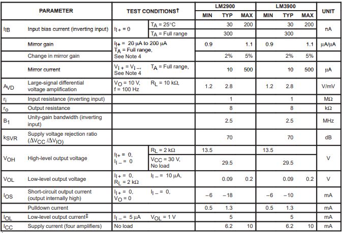
Ⅳ.Electrical Characteristics of LM3900,VCC=15 V,TA = 25°C(unless otherwise noted)
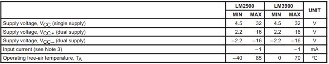
Ⅴ.Recommended Operating Conditions of LM3900
Ⅵ.Situations affecting the power supply voltage of LM3900
1.Performance degradation at low supply voltage: When the supply voltage drops close to the specified minimum operating voltage, the performance of the LM3900 may be affected. This may manifest as increased distortion of the output, reduced gain, or instability in other performance parameters.
2.The power supply voltage exceeds the specified range: If the power supply voltage of the LM3900 exceeds its specified operating range, it may cause unstable performance or even damage the chip. When using the LM3900, you should always follow the supply voltage specifications provided in the data sheet or specification sheet.
3.The offset voltage increases at low supply voltage: At lower supply voltage, the offset voltage of LM3900 may increase, which may have an impact on some precision applications.
4.Limitation of common-mode voltage range: The power supply voltage is also related to the common-mode input range of LM3900. If the common-mode voltage of the input signal exceeds the supply voltage range that the LM3900 can tolerate, it may cause undesirable common-mode effects and affect performance.
5.Supply voltage fluctuation: Instability or fluctuation in the supply voltage may also have a negative impact on the performance of the LM3900. Fluctuations in supply voltage can cause output signal instability, gain changes, or other performance issues.
Ⅶ.Pin configuration of LM3900
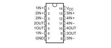
Pin1(1IN+):Non-inverting input 1
Pin2(2IN+):Non-inverting input 2
Pin3(2IN-):Inverting input 2
Pin4(2OUT):Inverting input 2
Pin5(1OUT):Output pin 1
Pin6(1IN-):Inverting input 1
Pin7(GND):Ground pin
Pin8(3IN-):Inverting input 3
Pin9(3OUT):Output pin 3
Pin10(4OUT):Output pin 4
Pin11(4IN-):Inverting input 4
Pin12(4IN+):Non-inverting input 4
Pin13(3IN+):Non-inverting input 3
Pin14(Vcc):Positive power supply voltage
Ⅷ.Performance of LM3900 at different temperatures
1.Temperature drift: Temperature changes may cause drift of some performance parameters, especially in high-precision or temperature-sensitive applications. For example, input bias current and offset voltage may change with temperature.
2.Supply voltage stability: Temperature changes may also affect the stability of the supply voltage, especially under extreme temperature conditions. This may cause distortion of the output waveform or other performance issues.
3.Common mode rejection ratio: At different temperatures, the common mode rejection ratio of LM3900 may change. In noise-sensitive applications, this is a factor to consider. Common-mode rejection ratio is an indicator of the ability of an operational amplifier to suppress common-mode signals. Ideally, an op amp should completely reject common-mode signals, but in reality, the common-mode rejection ratio is affected by a variety of factors, including supply voltage, temperature, packaging, and manufacturing processes. Therefore, the common-mode rejection ratio of the LM3900 may vary at different temperatures.
4.Frequency response: At different temperatures, the frequency response of LM3900 may also change. This may be important for high frequency applications or circuit designs requiring stable frequency response.
5.Gain changes: Temperature changes may cause gain changes, which may be critical to some amplifier circuit designs. At high temperatures, some electronic components may exhibit nonlinear behavior.
Frequently Asked Questions
1.How to ensure the stability of LM3900 under various working conditions?
Make sure that the power supply voltage of the LM3900 is within the specified range and that the power supply voltage is stable. Use a voltage regulator and appropriate power supply filtering circuitry to reduce noise and fluctuations in the supply voltage. Ensure input and output impedance matching in your design to avoid signal distortion and reflections. Consider using an appropriate buffer circuit or power amplifier to improve circuit stability.
2.What is the common mode rejection ratio of LM3900?
The common mode rejection ratio of the LM3900 is relatively high, usually above 60dB.
3.What is the difference between LM2900 and LM3900?
The LM2900 operates over the –40°C to 85°C temperature range, and the LM3900 operates over the 0°C to 70°C temperature range.